typoena.dev / hardware
Hardware wiring
Typoena is an ESP32-S3 with three things hanging off it: an e-ink panel, an SD card, and whichever USB keyboard you plug in. Everything below is what the firmware actually expects — if you are building one, this is the wiring.
Bring your own keyboard
There is no key matrix on the board and no keyboard in the bill of materials. The ESP32-S3 acts as a USB host, so any boot-protocol USB keyboard works — 60 %, 40 %, whatever you already type on. The port is wired VBUS-only: the machine sources 5 V to the keyboard rather than drawing from it.
One consequence worth knowing before you plug something in: because that port supplies power, it is not a port you connect a computer to.
Pin map
E-paper (SPI2, via DESPI-C579)
- GPIO 11
- MOSI
- GPIO 12
- SCK
- GPIO 7
- CS
- GPIO 6
- D/C
- GPIO 5
- RST
- GPIO 4
- BUSY (active high)
microSD (SPI3, its own bus)
- GPIO 14
- SCK
- GPIO 15
- MOSI
- GPIO 13
- MISO
- GPIO 10
- CS
Keyboard (native USB host)
- GPIO 20
- USB D+
- GPIO 19
- USB D−
Power
- GPIO 40
- PWR_HOLD — holds the soft latch on
- GPIO 41
- PWR_SENSE — reads the switch
- GPIO 1
- Battery sense (must be ADC1)
- GPIO 21
- CHRG — charger status
GPIO 26–37 are taken by the flash and octal PSRAM, and 43/44 are the console UART. Nothing else may use them.
Power path
The panel switch does not cut power. It is a signal: closing it pulls a latch gate low, the boost converter comes up, and the firmware asserts PWR_HOLD to hold itself on. Flipping it off does not drop the rail either — the firmware notices, saves, unmounts the card, paints a sleeping Typo on the screen, and only then releases the latch.
That last part is the whole reason for the design. E-ink keeps its last frame with no power, so a machine that dies mid-sentence leaves the screen lying about it. Here the screen is the power indicator: sleeping Typo means off, anything else means on.
Underneath sits a load-sharing stage so that a plugged-in machine runs from mains while the cell charges untouched, instead of micro-cycling the battery. Pull the cable and a body diode carries the load until the FET catches up — no brownout, nothing for the firmware to handle.
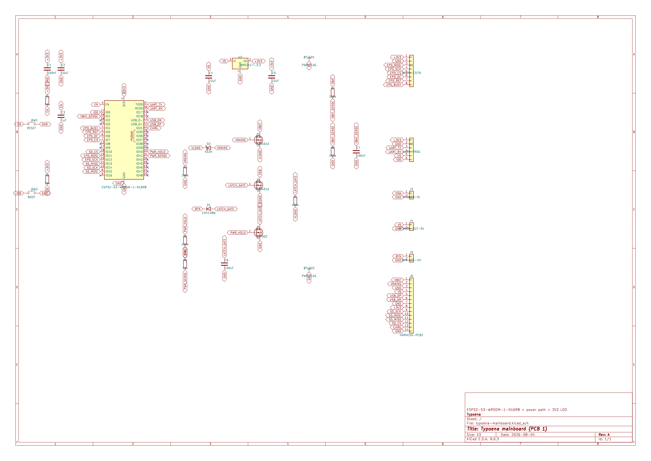
Mainboard schematic
The board carrying the module, the 3.3 V regulator and the power path. Connections are made by net label rather than drawn wires, so follow the names.
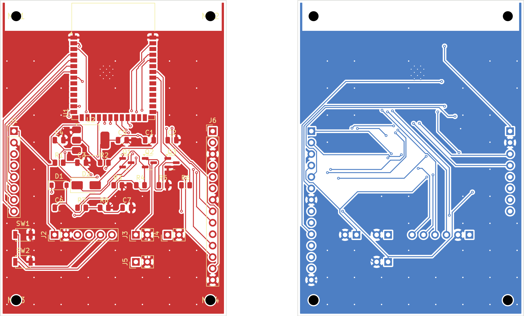
The copper
Two layers, both poured with ground. Front on the left, back on the right (mirrored, as you would look through the board). The blank band across the top is deliberate: the module's antenna sits there, and copper underneath it would detune the radio.
The second board — microSD, the two USB-C ports and the charger — is still on paper. Both live in the repo.